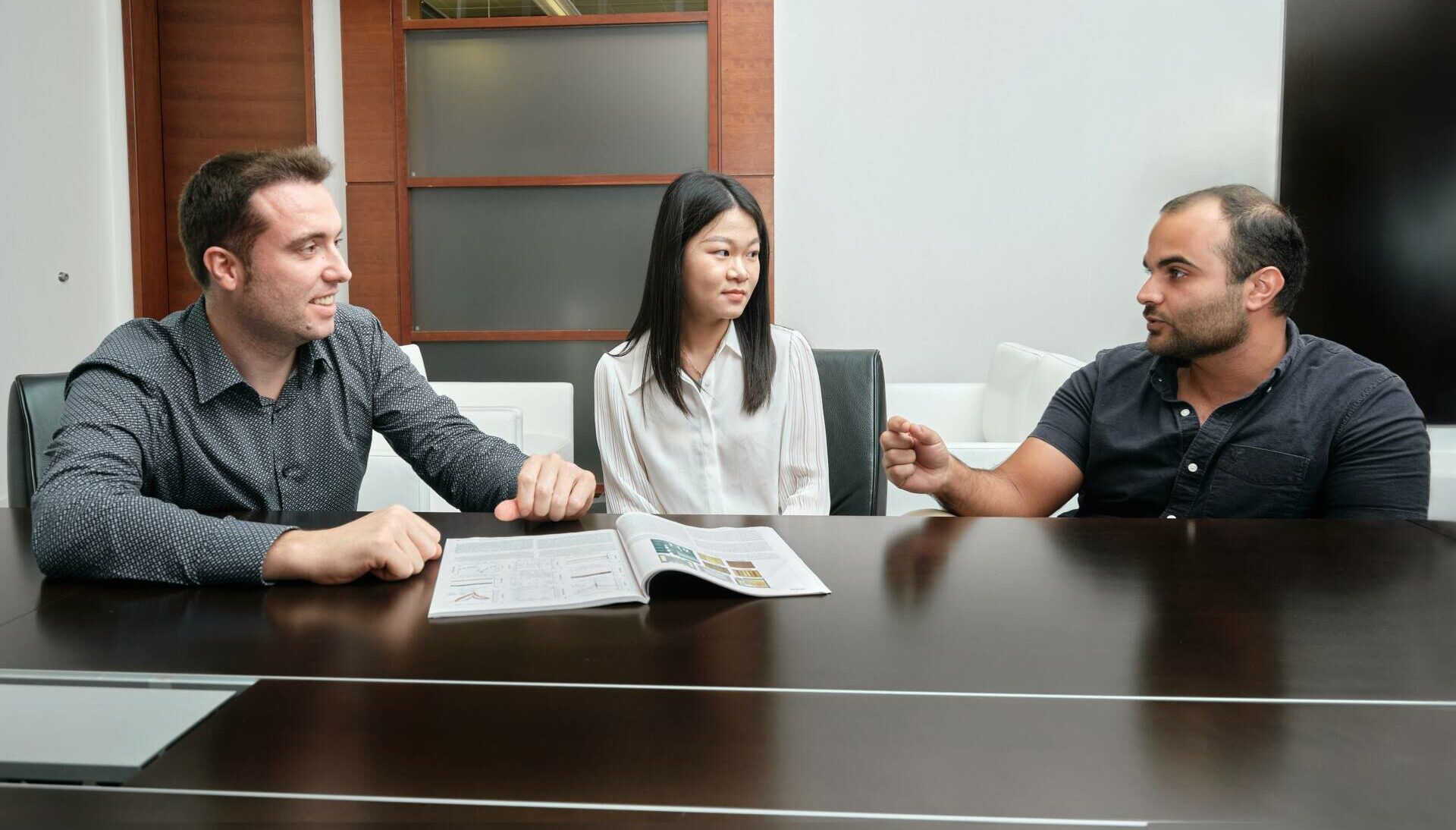
Of the elements that comprise a successful academic research group, the students are an essential component, the lifeblood of the endeavor. And, for students, being part of a strong team can have a big impact on their student experience.
“I’m always looking for potential students to join my group,” says Mario Lanza, a materials scientist working on 2D nanomaterials for electronic devices. “As professors at KAUST, we work very hard to attract the best students,” he adds.
Lanza has assembled a hard-working and vibrant bunch.
“One of the best things about being a student in Mario’s group is the diversity within the team in both cultural and scientific backgrounds,” says Ph.D. student Osamah Alharbi. “It makes conversations and scientific discussions really interesting,” he says.
In Lanza’s group, discussions are focused on developing advanced electronic devices by incorporating high-performance 2D nanomaterials into microchip design. Chips are assembled from a combination of conductor, semiconductor and insulator materials, which combine to control flow of electric charge. Different 2D nanomaterials, with key advantages over conventional 3D materials, can be used to perform each of these roles.
“Two dimensional materials, such as graphene or MXenes, have a higher conductivity than metals,” Lanza says. “They also dissipate heat very well, are almost transparent and are flexible,” he adds. For the semiconductor component, which switches on and off in a chip, two-dimensional semiconductors are less leaky in the off state than their 3D counterparts.
“This will make your device switch faster and consume less power,” Lanza says. And 2D insulators, such as hexagonal boron nitride, in which the group specializes, can help overcome a problem called scattering and improve heat dissipation. “Electronic devices fail due to heat, so using these materials can extend the reliability of the device,” Lanza adds.
The challenge in the field is to incorporate these materials into electronic microchips while avoiding any tiny impurities or defects in the material that impair their performance. “We contribute to solving this problem in two ways,” Lanza says. “We try to understand it by developing new methods to characterize these defects, and we develop new types of devices that are defect tolerant.”
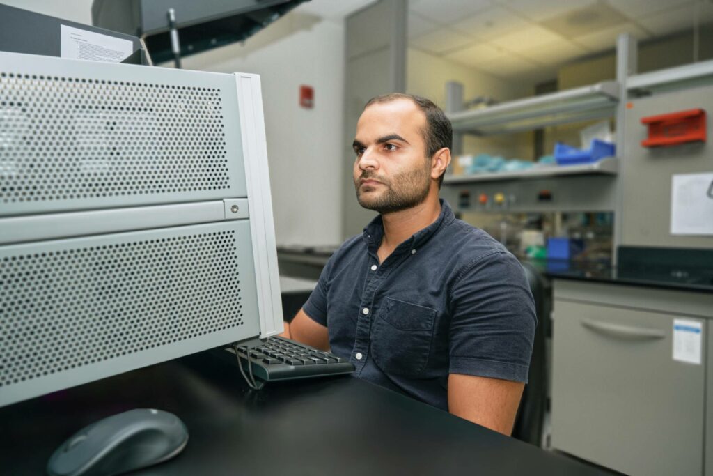
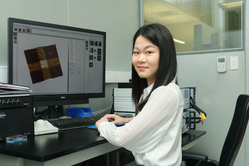
“The advanced characterization and fabrication instruments available at KAUST are a key drawcard for potential students,” says Yue Yuan, a Ph.D. student in Lanza’s group.
“There are many things that attracted me to KAUST — including its safe, pleasant environment by the Red Sea — but what attracted me most was the wonderful research conditions and advanced experimental equipment at KAUST,” she says. “Students get the opportunity to receive detailed training on these nice instruments. Using them is very helpful to the progress of our research projects,” she adds.
Gaining hands on expertise in cutting-edge instruments can help students in the next steps of their career path, Lanza notes. “I always tell my students that you have to be strong in everything and very strong in something,” he says. “We have to master all nanofabrication and nanocharacterization techniques — but in our group we are one of the world leaders in a technique called scanning probe microscopy, which we use to make 3D electrical maps of our materials.”
The team is beginning to receive inquiries from industry, he adds. “I see for the first time that the industry is looking for people like me who are working in these 2D materials. That’s very exciting,” Lanza says. “This work at KAUST, in partnership with other bodies such as King Abdulaziz City for Science and Technology, could help enable Saudi Arabia to establish its own niches in advanced circuit design and manufacture,” he says.
“Working in Mario’s group allows us to work on frontier problems in terms of novel materials and hardware structures that are not widely commercialized yet,” Alharbi says. “We’re pushing the limits of our field and gaining the experience that the industry might need in the future.”